So there were a pile of pictures of the DAS (Data Acquisition System) and BLASTbus electronics on my personal camera that I’ve finally gotten around to uploading. There are a lot more than these few I’ve posted, but others probably don’t find them as interesting as I do. I’m biased because I’ve been working on this for most of the past year.
These revamped BLASTbus electronics (BBus2, if you will) are in a wide variety of ways better than the old ones. The architecture is modular with a motherboard handling processing and BLASTbus communication, and a variety of daughter cards for all your digital or analog input/output needs. There are four varieties of daughter card so far. I’m especially attached to the digital daughter card because I had a much larger hand in making it (it is mostly the work of myself and Ian Hincks, an undergraduate that worked with me last summer).
I’m similarly attached to a new DAC system I/Ian/Barth developed. The digital daughter card uses a 5-bit address and 3 serial lines to talk to either 5 or 32 DACs depending how fancy one wants to be. BLAST doesn’t want to be fancy, so it just uses 5. RS-485 transmitters are used to make sure the digital signal doesn’t get corrupted over long wires.
-
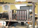
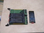
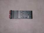
- An unpolished but functionally complete (!) BLAST DAS
-
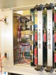
- DAS Innards show power supplies, backplane, and in the front DAC transmitter
-
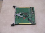
- Top side of motherboard shows the DSP
-
- Bottom of Motherboard, daughters attach to this side
-
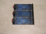
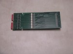
- Motherboard with three analog cards
-
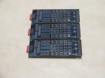
- All three analog varieties. Can you spot all the differences?
-
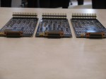
- The bottom of the analog cards. More differences here.
-
- Business ends of all the analog cards
-
- Top of digital daughter card. Aren’t white ICs pretty?
-
- Bottom of digital daughter.
-
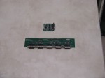
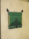
- BLAST-style individual DAC and transmitter
-
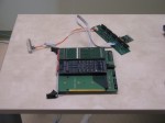
- Complete DAC system, minus crate
Leave a Reply